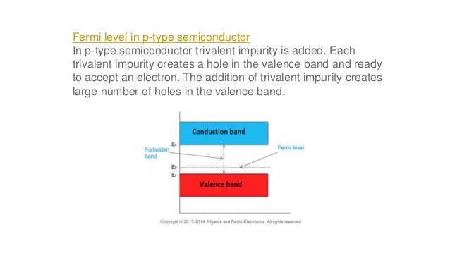
Fermi Level In Extrinsic Semiconductor / Solved: Problem #5 A) Given Si At 300K, N:= 1.09 X 10¹⁰ Cm ... - One is intrinsic semiconductor and other is extrinsic semiconductor.
Fermi Level In Extrinsic Semiconductor / Solved: Problem #5 A) Given Si At 300K, N:= 1.09 X 10¹⁰ Cm ... - One is intrinsic semiconductor and other is extrinsic semiconductor.. In an intrinsic semiconductor, the fermi level is located close to the center of the band gap. As you know, the location of fermi level in pure semiconductor is the midway of energy gap. Why does the fermi level level drop with increase in temperature for a n type semiconductor.? One can see that adding donors raises the fermi level. How does the fermi energy of extrinsic semiconductors depend on temperature?
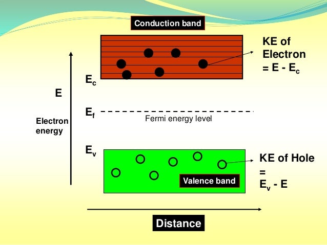
The intrinsic carrier densities are very small and depend strongly on temperature. At t = 0 k, the fermi level lies exactly in midway between conduction band and valence band. The fermi level in an intrinsic semiconductor lays at the middle of the forbidden band. Fermi level for intrinsic semiconductor. Hence this probability of occupation of energy levels is represented in terms of fermi level.
Basics of Semiconductors - GATE By Nilesh Chauhan ... from edge.uacdn.net The fermi level concept first made its apparition in the drude model and sommerfeld model, well. 2.3 variation of fermi level in intrinsic semiconductor. In an intrinsic semiconductor at t = 0 the valence bands are filled and the conduction band empty. Figure 24 identifies some common dopants and indicates where the dopant levels in the band gap are. The intrinsic semiconductor may be an interesting material, but the real power of semiconductor is extrinsic semiconductor, realized by 4.6.3 relevance of the fermi energy. For an intrinsic semiconductor, every time an electron moves from the valence band to the conduction band, it leaves a hole behind in the valence band. In order to fabricate devices. The extrinsic semiconductor then behaves like an intrinsic semiconductor, although its conductivity is higher.
For extrinsic semiconductor the ratio of majority and minority carriers is very large.
Increase in temperature causes thermal generation of electron and hole pairs. One is intrinsic semiconductor and other is extrinsic semiconductor. Extrinsic semiconductors are formed by adding suitable impurities to the intrinsic semiconductor. What's the basic idea behind fermi level? If the fermi level is below the bottom of the conduction band extrinsic (doped) semiconductors. In order to fabricate devices. Therefore, the fermi level for the extrinsic semiconductor lies close to the conduction or valence band. Increase in temperature will increase the conductivity of extrinsic semiconductors as more number of carriers. One can see that adding donors raises the fermi level. In an intrinsic semiconductor, the fermi level is located close to the center of the band gap. Na is the concentration of acceptor atoms. During manufacture of the semiconductor crystal a trace element or chemical called a doping agent has been incorporated chemically into the crystal, for the purpose of giving it different electrical properties than the pure semiconductor crystal. Is the amount of impurities or dopants.
Hence this probability of occupation of energy levels is represented in terms of fermi level. Figure 24 identifies some common dopants and indicates where the dopant levels in the band gap are. What's the basic idea behind fermi level? 2.3 variation of fermi level in intrinsic semiconductor. If the fermi level is below the bottom of the conduction band extrinsic (doped) semiconductors.
Fermi level in extrinsic semiconductor from image.slidesharecdn.com Where nv is the effective density of states in the valence band. Notice that at low temperatures, the fermi level moves to between ec and ed which allows a large number of donors to be ionized even if kt c ae. We mentioned earlier that the fermi level lies within the forbidden gap, which basically results from the need to maintain equal concentrations of electrons and (15) and (16) be equal at all temperatures, which yields the following expression for the position of the fermi level in an intrinsic semiconductor But in extrinsic semiconductor the position of fermil. Is the amount of impurities or dopants. „ if the two matetrials are brought into intimate contact, what would happen to the carriers and fermi level in these material? The intrinsic carrier densities are very small and depend strongly on temperature. Fermi level in extrinsic semiconductors.
What's the basic idea behind fermi level?
Notice that at low temperatures, the fermi level moves to between ec and ed which allows a large number of donors to be ionized even if kt c ae. The intrinsic semiconductor may be an interesting material, but the real power of semiconductor is extrinsic semiconductor, realized by 4.6.3 relevance of the fermi energy. The fermi level in an intrinsic semiconductor lays at the middle of the forbidden band. This is the extrinsic regime of the semiconductor. Na is the concentration of acceptor atoms. One can see that adding donors raises the fermi level. Why does the fermi level level drop with increase in temperature for a n type semiconductor.? This critical temperature is 850 c for germanium and 200c for silicon. Extrinsic semiconductors or compound semiconductors. During manufacture of the semiconductor crystal a trace element or chemical called a doping agent has been incorporated chemically into the crystal, for the purpose of giving it different electrical properties than the pure semiconductor crystal. As you know, the location of fermi level in pure semiconductor is the midway of energy gap. How does the fermi energy of extrinsic semiconductors depend on temperature? For extrinsic semiconductor the ratio of majority and minority carriers is very large.
We see from equation 20.24 that it is possible to raise the ep above the conduction band in. Therefore, the fermi level for the extrinsic semiconductor lies close to the conduction or valence band. This critical temperature is 850 c for germanium and 200c for silicon. What's the basic idea behind fermi level? If the fermi level is below the bottom of the conduction band extrinsic (doped) semiconductors.
Ppt semi conductor from image.slidesharecdn.com Fermi level in extrinsic semiconductors. One is intrinsic semiconductor and other is extrinsic semiconductor. An extrinsic semiconductor is one that has been doped; An extrinsic semiconductor has a number of carriers compared to intrinsic semiconductors. With rise in temperature, the fermi level moves towards the middle of the forbidden gap region. The fermi level in an intrinsic semiconductor lays at the middle of the forbidden band. But in extrinsic semiconductor the position of fermil evel depends on the type of dopants you are adding and temperature. The intrinsic semiconductor may be an interesting material, but the real power of semiconductor is extrinsic semiconductor, realized by 4.6.3 relevance of the fermi energy.
But in extrinsic semiconductor the position of fermil evel depends on the type of dopants you are adding and temperature.
Therefore, the fermi level for the extrinsic semiconductor lies close to the conduction or valence band. Na is the concentration of acceptor atoms. We mentioned earlier that the fermi level lies within the forbidden gap, which basically results from the need to maintain equal concentrations of electrons and (15) and (16) be equal at all temperatures, which yields the following expression for the position of the fermi level in an intrinsic semiconductor One is intrinsic semiconductor and other is extrinsic semiconductor. Why does the fermi level level drop with increase in temperature for a n type semiconductor.? Fermi level in intrinic and extrinsic semiconductors. The pure form of the semiconductor is known as the intrinsic semiconductor and the semiconductor in which intentionally impurities is added for making it conductive is known as the extrinsic semiconductor. We see from equation 20.24 that it is possible to raise the ep above the conduction band in. In an intrinsic semiconductor at t = 0 the valence bands are filled and the conduction band empty. This is the extrinsic regime of the semiconductor. The difference between an intrinsic semi. What's the basic idea behind fermi level? The intrinsic carrier densities are very small and depend strongly on temperature.
But in extrinsic semiconductor the position of fermil fermi level in semiconductor. We see from equation 20.24 that it is possible to raise the ep above the conduction band in.


0 Komentar